minimize signal distortion in RF PCBs
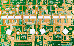
Printed Circuit Boards (PCBs) are the backbone of modern electronic equipment and are responsible for transmitting and dissipating current while keeping components at optimal performance. RF PCBs are unique in that they are able to carry and process high-frequency signals, and require special considerations when designing them. This includes minimizing signal distortion, noise suppression, and impedance matching. It’s also essential to properly route RF signals on the PCB to avoid unwanted interference.
In RF PCBs, the higher frequency of the signals causes the copper pathways to heat up at a faster rate, which in turn increases the amplitude of the EM fields. These heightened EM fields can cause unwanted interference and signal degradation. This is why RF PCBs are more susceptible to issues like EMI and crosstalk than standard PCBs. This makes it even more important to use proper design practices and follow specialized rf pcb guidelines during the layout and design process.
To minimize the effects of EMI, RF PCBs should use shielding techniques that effectively block electromagnetic waves from passing through the circuit. Moreover, it’s important to select the right materials for an RF PCB. This includes choosing the right substrate material, layer sacking, and trace width. Additionally, it’s recommended to use non-conductive materials like aluminum nitride and alumina when making an RF PCB.
A specialized RF PCB can improve the efficiency of an RF signal by reducing interference and increasing power transfer. This type of specialized PCB can be used in applications like wireless communication and radar systems, which rely on the efficient transmission of high-frequency signals.
Minimizing signal distortion in RF PCBs is essential for ensuring reliable operation of these high-frequency electronic devices. This can be achieved through impedance matching, reducing noise and crosstalk, and minimizing electromagnetic interference (EMI).
How do you minimize signal distortion in RF PCBs?
One of the most critical factors in maintaining signal integrity is choosing the correct dielectric thickness for an RF PCB. Depending on the desired RF frequency, different dielectric materials can have different losses. This is why a thorough analysis of the PCB design is required to determine the best dielectric material for the job.
Moreover, the characteristics of the substrate material can influence its ability to absorb or dissipate heat. In addition, the thickness of the board’s conductive layers can also affect the signal’s characteristic impedance. The characteristic impedance of a transmission line can be optimized by using techniques such as shunt or series impedance matching, in which a capacitor or inductor is placed in parallel with the source or load, respectively.
Another method for minimizing signal distortion is to keep the traces as short as possible, which can be accomplished by using stitching vias and avoiding unnecessary vias. Vias can cause what is known as parasitic capacitance, which leads to attenuation. Lastly, a low-pass filter can be used to reduce the distortion of the RF signal and ensure a clear transmission.
Finally, RF PCBs should be designed with the RF traces on the top layer and the ground plane on the bottom to prevent the RF and non-RF components from interfering with each other.